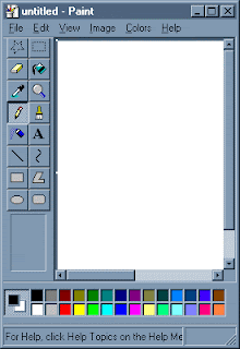
I recently had an inquiry about using 'MS Paint' for drawing PC board layouts. Although there are several freeware programs available for designing and drawing PC layouts, the ones I have tried had onerous learning curves. I also found that unless I was designing boards fairly regularly, I would have to go back and re-learn many of the functions each time I used the program. If you are regularly making a lot of boards, then these programs are certainly the way to go as they are packed with every feature you might need.
On the other hand, MS Paint meets all of my requirements and is simple to use ... I like simple. Although some might turn up their noses at MS Paint, I have found it to be a powerful and underestimated software tool. Here are some of the things that you might want to remember if drawing a PC layout with 'Paint'.
1. Take the time to read the built-in HELP and USING files. It doesn't take long to learn all of the functions along with some of the shortcuts.
2. Always draw with the IMAGE ... DRAW OPAQUE function turned off (unchecked). Do this first. This way, lines can go as close as you want without any blocking or overlapping. Try it the other way and you can see what happens.
3. If you are working with IC's, take the time to make a 'master' pattern that can be saved and copied anytime that you need it. A 16-pin layout can by used for 14 and 8 pin IC's by copying and pasting it and then erasing the unwanted pins.
4. Similarly, once you have established the correct pad spacing for certain capacitors or resistor sizes, copy and save them for future use. Finding the correct spacing will require a few trial printouts so you can measure the exact gap. This works great for SMD components as well.
5. For detailed work, use the VIEW ... ZOOM...CUSTOM function to magnify the layout. This also allows you to use a grid if you find this helpful.
6. Never SAVE your layout while in ZOOM mode as you can't go back to the original size when you re-load your plan. I learned this the hard way.
7. For drawing perfectly straight lines, squares or round circles, hold the SHIFT key down when drawing the element.
8. For large areas of copper (groundplanes), outline the area then choose the FILL symbol to create the area.
9. With a little planning, you can almost always avoid jumpers to make a crossover connection, unless your circuit is very complex.
10. When you make a mistake, just use the EDIT ...UNDO command. You can go back several steps with this helpful function.
11. I will often draw a thin line between to pads to see if they are on the same level ... and then UNDO the line once I have checked.
12. Always SAVE your layout as a Monochrome Bitmap with the FILE ... SAVE AS function. Using some of the other modes will create less than solid blacks and some random pixels that can lead to etching problems.
13. If using the 'toner iron-on' method of etching, set your printer options to the highest resolution (mine is 1200 dpi) and then choose the darkest 'print' option. You want as much toner thickness as possible. Note that this method works only with laser / toner printers and not the ink-jet / bubble types.
14. For the iron-on transfer paper, I have had good success with the shiny yellow transfer paper widely available on E-Bay, usually with free shipping. I get the best results when pre-heating the PCB in the toaster oven before ironing-on the pattern ... not too hot to touch however.
If you just build the occasional PC board, you might find using MS Paint worthy of a try. It has been meeting my needs for many many years and once you have done a few, unlike some PC software, it doesn't take long to build a new board without having to learn how to use it all over again.


No comments:
Post a Comment